Table Of Content
When selecting a design package to use, it is always advisable to use some of the latest tools with available support and community. In the EDA industry, some of the best and most popular tools are mostly not free. In this article, I will highlight some of the best free PCB design software you can find for designing your printed circuit board layout, and hopefully, this list will help you to pick what works for you. PCB design software can help you design your printed circuit boards easily and efficiently while saving significant time and resources. It will also help you check your design’s performance and fix it in the early stages so you can send only high-quality designs into the production stages.
What factors should be considered while choosing PCB design software?

The classic way of sending a board layout to a manufacturer is by creating Gerber files from your design. But some (ex. OSH Parks) also accept KiCad files directly so that you don’t have to do any conversion. Zachariah Peterson has an extensive technical background in academia and industry. He currently provides research, design, and marketing services to companies in the electronics industry.
With 14.8% CAGR, PCB Design Software Market Size to Surpass USD 8.52 billion by 2030 - GlobeNewswire
With 14.8% CAGR, PCB Design Software Market Size to Surpass USD 8.52 billion by 2030.
Posted: Wed, 13 Dec 2023 08:00:00 GMT [source]
Step 2: Draw Your Schematics
Their design will go through the testing phase, where engineers will verify the performance and feasibility of the PCB designs. And manually testing PCB designs is a hassle, labor-intensive, and time-consuming process. It also may involve inaccuracies that can result in serious design flaws and deteriorate final product quality. Hence, PCB design software helps you make this PCB designing process easier, faster, cost-effective, and efficient.
Digitally integrated & optimized
Your feedback matters to us, so we’ve made changes based on your input. And to make life easier, we’ve adjusted our order cut-off time to 3pm Pacific time for all manufacturing services. Don’t complicate things by using multiple vendors to get finished boards. This makes it a huge pain to keep the width of your traces consistent, especially as they get narrower. To properly power your ICs, we recommend using common rails for each supply. Also, be sure to use solid and wide traces to let that power easily flow through to your energy-hungry ICs, and avoid daisy-chaining power lines between parts to prevent any voltage drop issues.
Designed by Novarm, DipTrace aims to bring full PCB design options and functionality while keeping the experience simple and intuitive. But with over three decades of development and countless improvements over the years, it’s a powerful PCB design tool that rivals many of the paid options. Suitable applications include single-board computers, motor controllers, custom mechanical keyboards, drones, smartwatches, low-power cameras, and much more. By following the above PCB design steps, the process of creating a comprehensive PCB board design is as easy as counting to ten. Using a systematic approach such as this ensures that all aspects of your circuit board design are accounted for inherently during the process, with minimal need to retrace your steps.
OrCAD – Dynamic PCB Software Used by Apple, Free for Students
This allows you to download and use the software for free if you’re a student, and there are also plans for teachers and universities. PADS even hosts a unique program that can provide eligible startups with discounted access to PADS Profesional, which is certainly worth considering if you have a young business that relies on layout PCB software. Autodesk offers fantastic support and learning resources for Eagle, and it’s one of the most widely compatible CAD PCB software, being available on Mac, Windows, and Linux. Overall, it’s probably the most comprehensive and highest quality PCB design solution money can buy.
CircuitMaker – Best Free PCB Design Software for Beginners & Windows
When you transfer your schematic information to the PcbDoc the component footprints are shown in addition the board outline specified. Prior to placing components you should define the PCB layout (i.e. shape, layer stackup) using the Layer Stackup Manager, shown below. Verify the changes (addition of the SchDoc information to the project without error) by clicking on the Validate Changes tab. If the status for all items is green, then click on the Execute Changes tab. Altium Designer can save you a substantial amount of time during this PCB design step. However, John Teel, the electronics design expert on the PredictableDesigns.com blog finds the EAGLE graphic interface both complex and not user-friendly.
3D Printing Industry Statistics (2024 Update)
Its PCB editor is easy enough to make designing easy even if you are new to the software. You can export industry-standard files such as DXF and Gerber to complete your design flow (schematic to layout). Furthermore, Ultiboard provides many electronic solutions so that you will never be left behind while designing and manufacturing your electronic components. Use a simple spreadsheet-based interface to enter and manage your PCB design rules. The PCB layout tools are similarly intuitive, with helpful alignment tools and real-time synchronization to ensure your schematic and layout designs are always in sync. It uses interactive push and shove routing with obstacle avoidance features and tools for completing loop removal, cornering, and other functions quickly.
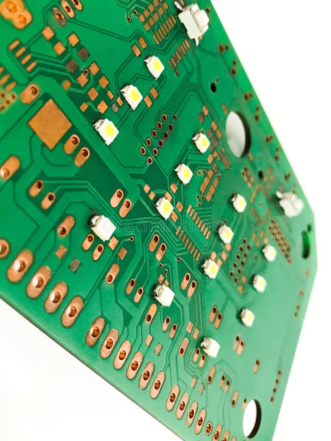
After the official birth of commercial EDA since 1981, different design software as been produced from the EDA industry. Printed Circuit Boards, also known as PCBs, are the foundation of any hardware-based product. Before EDA software, Engineers usually designed electronics circuitry and integrated circuits by hand or some other manual process. This process allows for several paths to more sustainable, circular PCB lifecycles. Damaged circuit boards, such as those with cracks or warping, can, in some cases, be repaired.
You’ll want to keep these components away from other parts that are heat sensitive, such as thermocouples and electrolytic capacitors. If those capacitors get too hot, they’ll start to lose their ability to retain a charge. Send your product to manufacturing in a click without any email threads or confusion. We have only scratched the surface of what is possible to do with Altium Designer on Altium 365. You can check the product page for a more in-depth feature description or one of the On-Demand Webinars. The CircuitMaker Community makes working together, sharing designs and iterating easier than ever.
Connect your ECAD solution with the most popular MCAD tools, Ansys simulation experts, and PLM systems to seamlessly exchange data and reduce costly and time-consuming rework. Bring together all aspects of your electronics design in one place to help you deliver better products faster than ever before. Downloading PADS software is easy – simply create an account, visit the download page, select which version you want, click the download button and follow the instructions. Altium Designer, OrCAD, and Eagle are the three PCB design software that are most widely used in industry and by leading tech companies. The cost of the best PCB software varies greatly, from free programs like CircuitMaker to professional solutions like Altium Designer that cost more than $300 a month.


No comments:
Post a Comment